
$24
Lab #8: Decoder Solution
Objectives:
In this experiment, you will use the decoder to implement some logic functions.
IC chips:
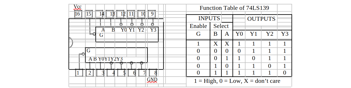
- One 74LS139 chip (DUAL 2 4 decoder with negated output and zero-enable).
- One 74LS20 chip (DUAL 4-input NAND gates).
The decoder chip you will use in this lab is the 74LS139, which contains two sets of 2 4 decoder with negated outputs and zero-enable. The pin configuration and the function table are given below.
The 74LS20 chip contains two 4-input NAND gates. The pin configurations are shown below.

Propagation delay:
Assume that the propagation delay for every NAND gate in 74LS20 is 15 ns (nano-seconds), and the propagation delay for each decoder in 74LS139 is 35 ns.
AY2019/20 Semester 2 - 1 of 3 - CS2100 Lab #8
Procedure:
- Given a 3-variable function S(P,Q,R) = (P + Q + R) (P + Q') (P' + R), write this function in the product-of-maxterms form, using the M notation.
S(P,Q,R) = M ( ____________________ )
2. Complete the truth table for S below.

- With the truth table above, implement function S using the 2 4 decoders in the 74LS139 chip, and NAND gates in the 74LS20 chip. Connect the inputs P, Q, and R to SW7, SW6 and SW5 on your logic trainer respectively.
Complete the following logic diagram.

- Show your implementation to your lab TA before you proceed to implement function F in step 7.
- What is the propagation delay of your circuit above? _______ ns.
- Given a 4-variable function F(W,X,Y,Z) = M(3, 7), write out the simplified SOP expression for F below.
Simplified SOP expression: F = ____________________
- Implement F using only ONE 2 4 decoder, without any additional logic gate. Connect W, X, Y and Z to SW7, SW6, SW5 and SW4 respectively. (You may find that you do not need to use all 4 inputs.) You circuit is considered wrong if it uses any additional logic gate, even though it produces the correct output.
Complete the logic diagram below.

- Show your implementation to your lab TA.
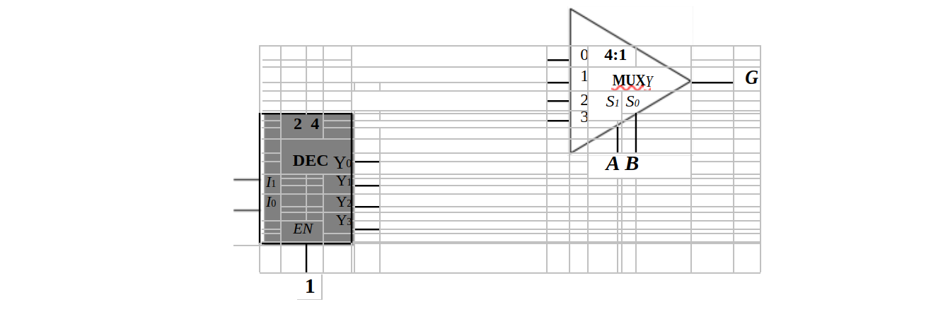
- Using one 4:1 multiplexer and one 2 4 decoder with 1-enable as shown below, show how you might implement function G(A,B,C,D) = m(0, 6, 9, 15) without using any additional logic gate. Complete the diagram below.
Note that the selector lines for the 4:1 multiplexer have been fixed to AB, and you must not change it.
You do not need to implement this since you are not given any multiplexer in this lab.
Marking Scheme: Report (18 marks), Circuit (7 marks); Total: 25 marks.
Your graded report will be returned to you at the next lab.